
Design

Materials and process design encompasses choosing correct device stacks, their interfaces, device geometry and doing multiple mask layer process design for semiconductor devices like Ferroelectric Capacitors, MOSFETs based on 2D semiconductors or oxide semiconductors, ferroelectric field effect transistors (FeFETs), ferroelectric tunnel junctions (FTJs) and so on.
Some recent results from the Devices:
Ferroelectric Hf-Zr-O devices show large remanent polarization and endurance exceeding 1 billion switching cycles. [1] Integrating them in a crossbar array design will enable their use in parallel information processing within In-memory Computing (IMC) paradigm.
[1] Understanding fatigue and recovery mechanism in Hf0. 5Zr0. 5O2 capacitors for designing high endurance ferroelectric memory and neuromorphic hardware, X Li, P Srivari, E Paasio, S Majumdar, Nanoscale 17, 6058 – 6071 (2025).
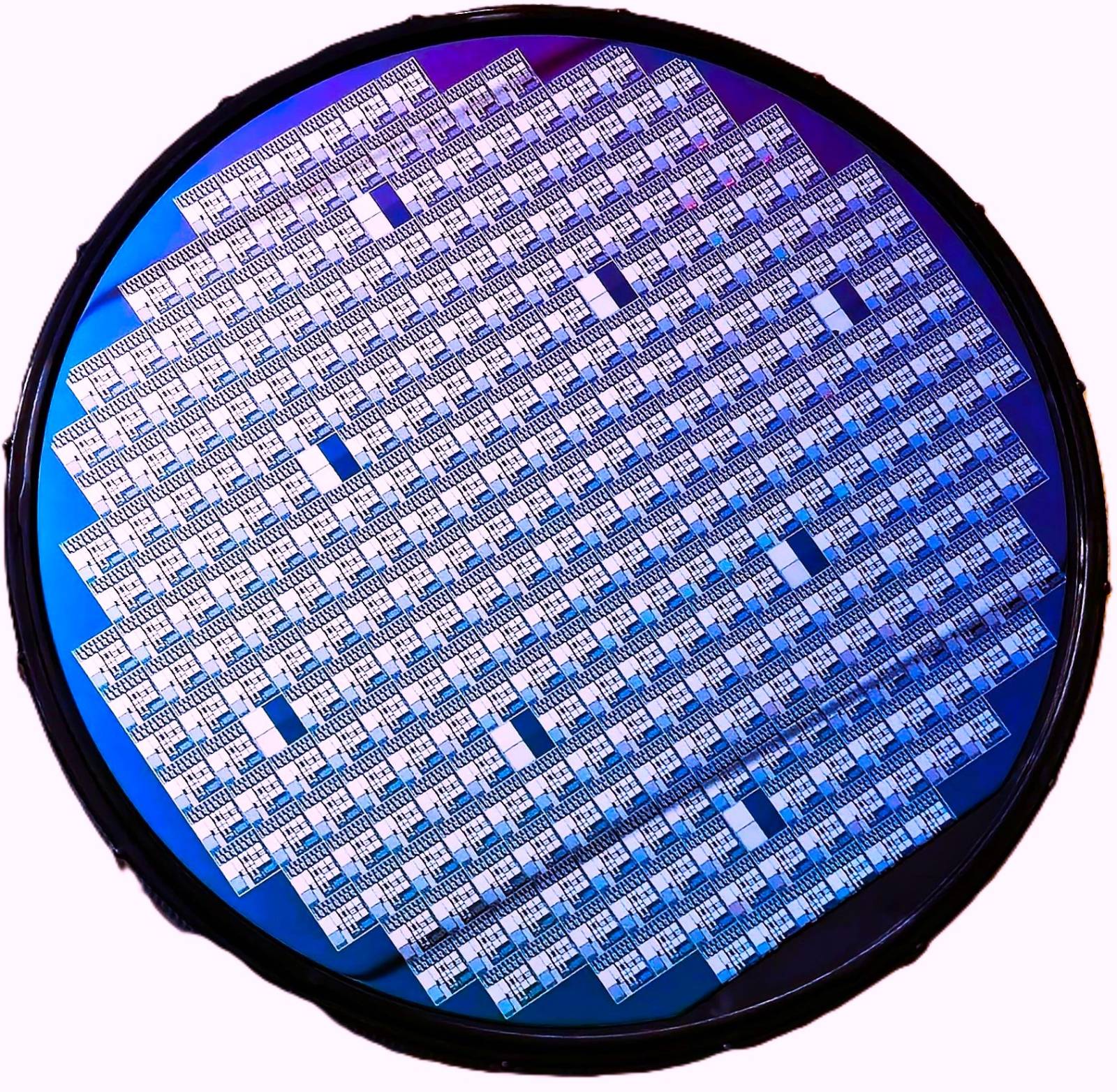
Fabrication

Device fabrication involves thin film deposition of metal, dielectric, ferroelectric and semiconductor layers followed by multi-mask layer processing using lithography (both dry and wet), etching and annealing steps. Dielectric and Ferroelectric layer fabrication involves atomic layer deposition (ALD) while metal evaporations use electron beam evaporation techniques. For lithography, both photolithography and e-beam lithography are used depending on criticality and dimensionality of the structures.
After the wafer processing is completed, chips are diced and packaged for their thorough electrical characterization. Rapid characterization cycle provides feedback to the design and fabrication team, helping process optimization.

Characterization

Fabricated devices are characterized for their electrical properties using ferroelectric material tester Aixacct 2000 and semiconductor parameter analyzer Keysight B 1500 with pulse modules capable of producing pulse of width down to 100 ns. Arbitrary pulse generator modules attached with the system enable designing of custom pulses required for characterizing advance memory devices and synaptic or neuron components. For understanding reliability and reproducibility of the fabricated components, we do thorough wafer-scale characterization and utilize machine learning (ML) tools for feature extraction.
For Chips JU project ARCTIC, we investigate Cryogenic Memories and for this purpose, we do device characterization down to 4 K.
Data Analysis and Modelling

We perform physics-based compact modelling to reproduce experimentally measured polarization switching data in ferroelectric thin film capacitors under different electric field and temperature conditions. Additionally, we investigate device-to-device variation effect on the model parameters to enable large-scale integration of the FE components to complex functional circuits. Due to increasing interest in cryogenic electronics for quantum computing and space technologies, effect of temperatures on polarization switching is investigated down to 4 K. [3] It is shown the model can reproduce the experimental polarization-voltage relation of Hafnium Zirconium Oxide capacitors with nearly 100% accuracy, for different electric fields and temperatures down to 4 K, including analog switching. It is find cooling the devices below 100 K increases polarization update linearity and symmetry significantly. This results represent an important advancement toward application of ferroelectric capacitors for large-scale memory and neuromorphic circuits operating down to deep cryogenic temperatures.
[3] A Physics-Based Compact Model for Ferroelectric Capacitors Operating Down to Deep Cryogenic Temperatures for Applications in Analog Memory and Neuromorphic Architectures, E Paasio, R Ranta, S Majumdar, Advanced Electronic Materials, 2400840 (2025).
Neuromorphic Simulation

Online training of deep neural networks (DNN) can be significantly accelerated by performing in situ vector-matrix multiplication in a crossbar array of analog memories. However, training accuracies often suffer due to nonideal properties of synapses such as nonlinearity, asymmetry, limited bit precision, and dynamic weight update range within a constrained power budget. We have developed a fully scalable process for digital and analog ferroelectric memory transistors with possibilities for both volatile and nonvolatile data retention and <4 V operation that would be suitable as programmable synaptic weight elements. Ferroelectric gate insulator and 2D semiconductor MoS2 as the n-type semiconducting channel material make them suitable for flexible and wearable substrate integration. The ferroelectric-only devices show excellent performance as digital nonvolatile memory operating at <±5 V while the hybrid ferroelectric–dielectric devices show quasi-continuous resistive switching resulting from gradual ferroelectric domain rotation. Analog conductance states of the hybrid devices allow good linearity and symmetry of weight updates and produce a dynamic conductance range of 104 with >16 reproducible conducting states. Network training experiments with these ferroelectric field-effect transistors show >96% classification accuracy with Modified National Institute of Standards and Technology (MNIST) handwritten datasets highlighting their potential for implementation in scaled DNN architectures. [4]

[4] Back-end and Flexible Substrate Compatible Analog Ferroelectric Field Effect Transistors for Accurate Online Training in Deep Neural Network Accelerators, S Majumdar, I Zeimpekis, Advanced Intelligent Systems 5 (11), 2300391 (2023).
Circuit integration

Memristive components are integrated in a circuit capable of associative learning in multi-sensor fusion scenarios. The circuit can enhance fault tolerance of autonomous vehicles by dynamically adapting to multi-sensor inputs, including camera, LiDAR, radar, and ultrasonic sensors. The proposed circuit dynamically reinforces patterns, allowing the system to retain decision-making capabilities even when certain sensors fail or provide incomplete data. The fault tolerance of the circuit is validated through error analysis, proving that accurate outputs are generated even with missing sensor inputs. The system demonstrates an average error of 6.98% across 10 critical driving scenarios, with a power consumption of ≈152 mW per scenario, confirming its robustness, energy efficiency and adaptability in case of sensor failures and under-performance. The response time of the circuit has been optimized from milliseconds to seconds, aligning with realistic human-like reaction times required for autonomous navigation. [5, 6]
[5] A Memristive Associative Learning Circuit for Fault-Tolerant Multi-Sensor Fusion in Autonomous Vehicles, K Bhardwaj, D Semenov, R Sotner, S Majumdar, Advanced Intelligent Systems, 2500215 (2025).
[6] Preventing False Activations in Autonomous Vehicles: A Memristive Associative Learning Approach with Selective Sensor Pairing, K Bhardwaj, D Semenov, R Sotner, S Majumdar, 2025 14th International Conference on Modern Circuits and Systems (MOCAST), pp. 1-4 (2025).