

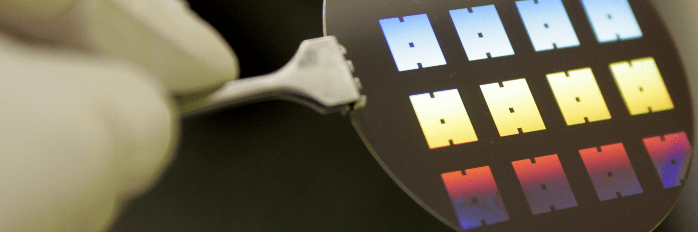
Fabrication
Device fabrications are done in Tampere University Cleanroom and Finland’s National Research infrastructure Otanano Micronova cleanroom. Details of the fab capabilities can be found in the respective links.
Details of the infrastructure can be found here:
Tampere University Cleanroom Facilities

National Research Infrastructure – Otanano Micronova
Characterization
Main characterization of the devices are done using Semiconductor parameter analyzer Keysight B1500 with pulsed module (waveform generator/fast measurement unit (WGFMU)) and Ferroelectric Material Tester (Aixacct TF analyzer 2000). For characterization of the devices under a large temperature window, a cryogenic probe station capable of measuring in the range of 4 – 350 K is utilized.
1. Semiconductor Parameter Analyzer

2. Ferroelectric Material Tester

3. Cryogenic Probe Station
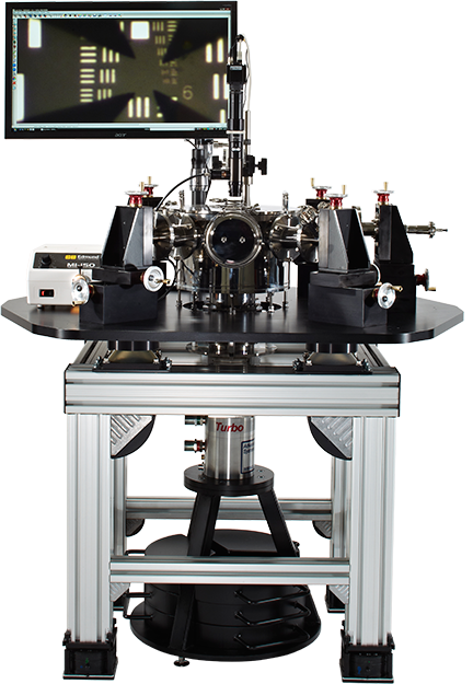 The Closed Cycle Cryogenic Probe Station provides a high vacuum cryogenic environment of up to <4 K – 350 K for measuring multiple devices consecutively without breaking vacuum or warming the system. The Probe Station contains 6 probes with 5 μm sensitivity, 2 inch measurement area, < 1 μm vibration levels, fast sample cooldown, custom wiring for DC, large optical access and optional 7:1 zoom microscope with ring light.
Emerging fields of Cryogenic Electronics and Quantum Technologies require electronics operating down to 4K. Main application of the system in our laboratory is characterization of semiconductor devices over a wide temperature range for properly understanding the device physics. Also optoelectronic characterization possibilities under a large range of temperature provides possibilities for exploring more fundamental physics.
A more comprehensive list of the infrastructure can be found at the Laboratory of Future Electronics webpage: Laboratory for Future Electronics
4. Tampere Microscopy Centre
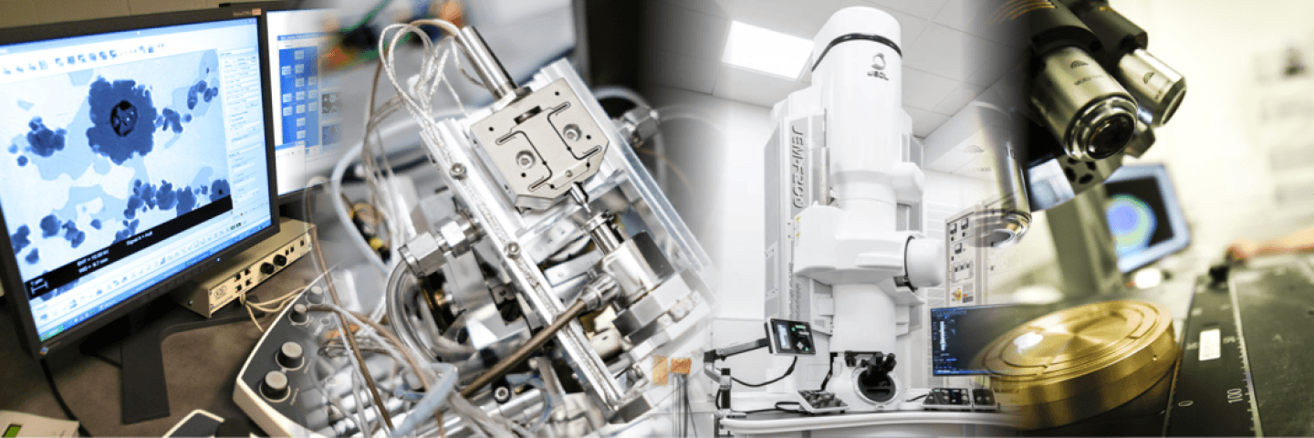
Details about the Tampere Microscopy Centre can be found here: Tampere Microscopy Centre

Extensive structural characterizations of the devices are done utilizing infrastructure of Tampere Microscopy Centre. It involves X.ray diffraction (XRD), Scanning electron microscopy (SEM), Tunneling electron microscopy (TEM), X-ray photoelectron spectroscopy (XPS) and atomic force and piezoforce microscopy (AFM & PFM respectively).