
SA/Intellisense
This project, jointly funded by Research Council of Finland (RCF) and National Science Foundation (NSF) develops near and in-sensor computing hardware. This project is an ongoing collaboration between TAU and University of Massachusetts Amherst.
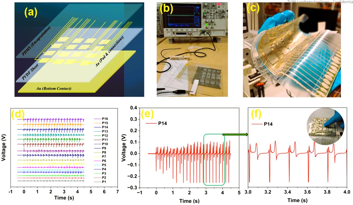
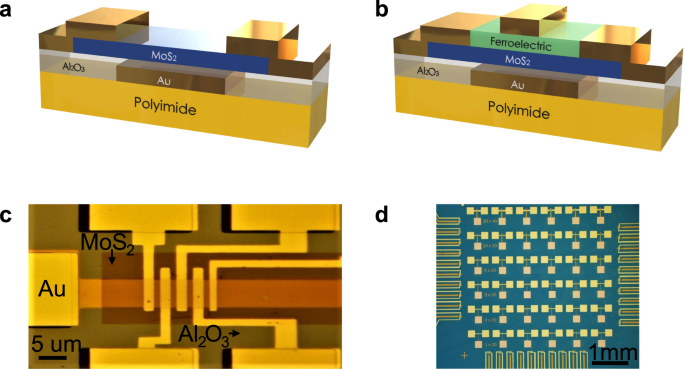
Project short description: Miniaturized sensor systems with in-built memory and computing function are the future of edge-AI. Currently sensing and computing happens in two different physical locations that needs huge amount of continuous data flow between the sensor and cloud computing platforms, causing unprecedented data traffic. This is unsustainable in terms of energy, time and capacity for processing sensor data and causes negative environmental impact of IoT applications.
The Intellisense project intends to go beyond the state-of-the-art by moving towards monolithically integrating sensing, memory and computing platform on a device level. This allows ubiquitous application of such sensor systems at low energy budget. Furthermore, building the platform on a flexible substrate further widens the scope of application of such systems in smart wearables making 24×7 vital-signs monitoring an affordable option.
SA/AI4AI
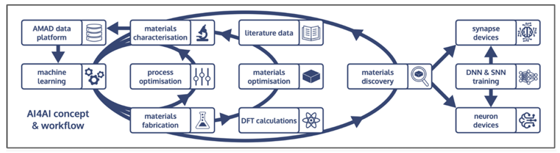
This project, funded by Research Council of Finland (RCF) investigates AI-software based Material design for sustainable AI hardware (AI4AI) development. This project is a collaboration between TAU and Aalto University, Finland.
Project short description: Artificial Intelligence (AI) tasks on digital von Neumann hardware is seriously challenging the conventional computation hardware in terms of speed and power consumption. Therefore, biologically inspired neuromorphic computing systems based on emerging memory devices, which combine storage and processing, are proposed as a viable solution. However, sustainable material based hardware development is often time consuming and expensive. The AI4AI project aims towards an AI based material design strategy for developing neuromorphic AI hardware that will be capable of performing AI tasks while operating at an extremely low power consumption in the order of fJ/bit. The research will demonstrate development of new hardware to bring neuromorphic computing to a level where proof-of-concept system demonstrates an ultra-low power operation without compromising the computational speed, accuracy, or learning capacity.
SA/Ferrari
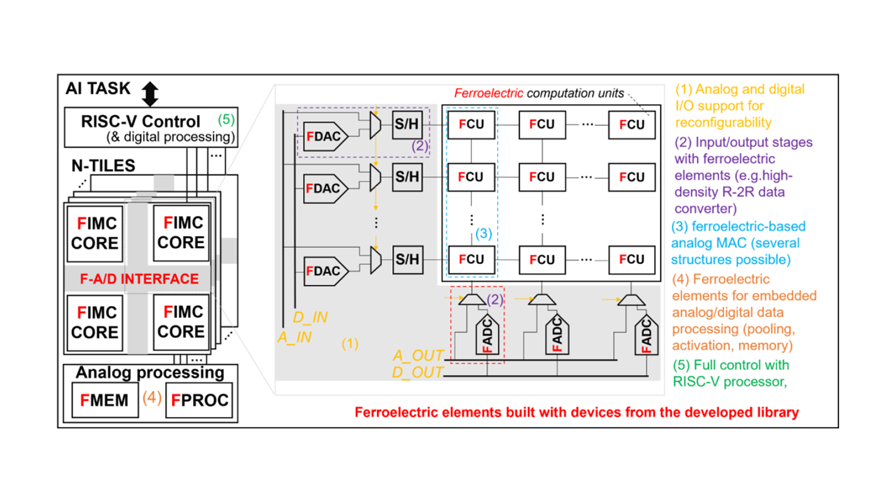
This project, funded by Research Council of Finland (RCF) investigates materials to devices to circuits for ultra-energy efficient neuromorphic edge devices. This project is a collaboration between TAU, Oulu University and Aalto University, Finland.
Project short description: A future driven by artificial intelligence (AI)-enhanced systems is expected to make our life easier, safer, or simply more entertaining. Yet, achieving these expectations in the realm of smart and interconnected devices (internet of things, 6G wireless communication, smart health monitoring, etc.) requires solving crucial challenges in the computation of AI models. In this project, we propose to investigate extremely energy-efficient neuromorphic computing, i.e., computing systems inspired by our brain, based on novel ferroelectric devices that are able to mimic biological computing mechanisms. We will create a library of these devices, fabricated and modelled, and ready to be integrated into typical computer-aided design tools used to design microelectronic systems. This also paves the way to building unique, multi-faceted neuromorphic expertise in Finland.
Chips JU_ARCTIC
ARCTIC is a large-scale European project funded by Chips JU.
The objective of ArCTIC is to bridge the void between quantum processors and their control electronics. ARCTIC will develop scalable, reliable, innovative control electronics for cryogenic quantum processors. The (cryogenic) technologies under development in ARCTIC will also have applications in several different fields from sensing to communication and will therefore lead to important cross-fertilization that will strengthen the forming European ecosystem on cryogenic classical and quantum microsystems. ARCTIC intends to establish a complete and comprehensive European supply chain for cryogenic photonics, microelectronics, and, in general, cryo-microsystems around the emerging quantum computing industry and different cryo-enabled ICT applications.
CMOS-and-Beyond team is leading the Cryogenic Memory and In-Memory Computing task in the project together with Industrial partners like Intel, Picosun/Applied Materials, and Okmetic, RTOs like Fraunhofer IPMS and VTT and academic partner like Lund University.
Doctoral Education Pilot project from PREIN flagship
The Doctoral Education Pilot project from PREIN flagship will investigate Photonic Neuromorphic Systems in collaboration with Optoelectronics Research Centre of Tampere University.
The fast development of brain-inspired neuromorphic computing systems has stimulated requirements for urgent developments of artificial synapses and neurons with ultralow-power consumption with capabilities for biologically plausible computing. In this doctoral study, photonic synaptic and neuron devices will be fabricated and characterized. In the artificial synaptic device, the incident light pulses would play the roles of action potentials, and the light-generated carriers would modify the pre-and post-synaptic membrane potential, similar to the neurotransmitter in biological synapses. Key synaptic functions, like photonic memory, multiple timescale synaptic plasticity, paired pulse facilitation and depression, dynamic “learning–forgetting” etc. will be investigated while for the photonic neurons, the task would be to identify and build systems that can integrate temporally-encoded pixel data at high speed and fire fast optical spikes upon detecting desired image features. Finally, the photonic system will be combined with a software-implemented neural network that will provide a full platform for complex image classification tasks.
PROFI8: Semiconductor technology (PHOTO-ELEC)
The PHOTO-ELEC profiling area combines expertise in photonics and microelectronics with the aim of developing more energy-efficient semiconductor technology. PHOTO-ELEC brings together fields related to semiconductor technology, for which Tampere University is already known worldwide.
Researchers in photonics, or the science of light, develop and produce light-based technologies and their applications. In microelectronics, very small electronic components and systems are studied and designed, particularly using semiconductors and optical components.
The synergy of these research fields and the strengthening of joint RDI (Research, Development, and Innovation) activities aim to meet the growing demand for advanced chips. The profiling area also includes new research infrastructure, such as the SiPFAB (System-in-Package Fabrication) pilot line for semiconductor chip packaging to be built in Tampere. The pilot line received significant funding from the European Commission and the Finnish government.
Related news: PHOTO-ELEC integrates photonics and microelectronics to develop more energy-efficient semiconductor technology
We are an Associated Partner in:
QuAHMET
The Euramet and European Commission funded project QuAHMET focusses on the traceable measurement and characterization of quantum anomalous Hall effect (QAHE) materials as devices and primary resistance standard candidates.
The specific objectives of the project are:
-
To improve the growth of magnetically doped topological insulator (TI), thin film samples, to explore the effects of anisotropic magnetic insulator layers and to produce high structural quality materials with properties optimized for the QAHE.
-
To investigate the bulk electronic, structural, magnetic, and magneto-electronic properties of the QAHE films and devices produced in Objective 1 under various temperatures (from below 50 mK up to 300 K), currents (from below 100 nA to over 1 µA) and applied magnetic fields (from 0 to 10 T) for different growth conditions. In addition, to investigate the limitations of QAHE, i.e., low critical temperatures and currents when working on precision growth-control of interfaces.
-
To investigate fabricated QAHE thin films and devices by surface sensitive scanning probes (SPM) and magnetometry techniques (e.g. Scanning SQUID, MFM, scanning SNOM) at low temperatures (from below 50 mK to 300 K), and to characterize their magnetic and structural properties using X-ray, and neutron investigations.
-
To develop and carry out detailed metrological assessments of QAHE devices .
-
To facilitate the take up of the technology and measurement infrastructure developed in the project by standards developing organizations, end users interested in applications, such as spintronics and topological quantum computing and advance the research and progress in the field of TIs.