
The PHOTO-ELEC profiling area combines photonics and microelectronics to develop increasingly high-performance and energy-efficient semiconductor solutions. These research and development efforts are supported by the €5.9 million grant awarded to Tampere University by the Research Council of Finland, aimed at strengthening the University’s research profile and advancing semiconductor expertise in Finland.
Semiconductors are found in almost all electronic devices, from TVs to smartphones. The semiconductor industry is globally significant, but the market is largely dominated by China, Taiwan and South Korea. Efforts are underway to promote both Europe’s and Finland’s self-sufficiency, competitiveness and sustainability in the semiconductor sector, such as the European Chips Act and the Chips for Europe initiative, which also involves Tampere University.
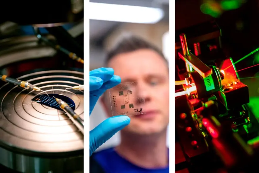
Tampere University’s PHOTO-ELEC profiling area brings together research fields related to semiconductor technology, building on the University’s international reputation for excellence in these domains. Researchers specialising in photonics – the science of light – develop light-based technologies and their applications, while microelectronics focuses on the study and development of tiny electronic components and systems, especially using semiconductors and optical components.
The efforts to foster synergies and advance research, development and innovation (RDI) activities in photonics and microelectronics are driven by the growing demand for advanced chips.
The integration of research fields creates synergy
The director of the PHOTO-ELEC profiling area, Professor Juha Toivonen from the Faculty of Engineering and Natural Sciences (ENS), explains that the convergence of photonics and microelectronics is a natural progression, as expertise in both fields is needed to develop increasingly energy-efficient semiconductors.
“With the PHOTO-ELEC project, we are exploring new research avenues and developing research activities at the interface between two faculties at Tampere University,” Toivonen says.
In photonics, electricity is needed to power light-based components, and light energy is converted back into electrical energy during the detection of light. Data is processed using microelectronic devices, but data transmission consumes a great deal of energy. Optical data transmission is more energy-efficient for large volumes of data.
Professor of Electronics Matti Mäntysalo, vice director of the PHOTO-ELEC project from the Faculty of Information Technology and Communication Sciences (ITC), also emphasises the synergies between photonic and microelectronic technologies.
“Microelectronics and photonics are manufactured similarly, using both micro- and nanotechnologies. The PHOTO-ELEC project will bring microelectronics closer to photonics and foster closer collaboration between ENS and ITC,” Mäntysalo says.
Design expertise is essential in microelectronics, but the actual fabrication of integrated circuits occurs outside of this domain. In contrast, photonics adopts a hands-on approach, with investments especially directed towards manufacturing facilities.
Investing in new professionals and equipment
Finland faces a growing demand for semiconductor professionals. The funding secured by PHOTO-ELEC will enable Tampere University to further advance its expertise in photonics and microelectronics by establishing new research groups and recruiting new tenure-track professors and other specialists.
“The development of a strong research profile will not only help to clarify this field of expertise but also attract new professionals to an industry that urgently needs them. While the project is research-driven, it will also have an impact on teaching and education, including the training of doctoral students,” Mäntysalo notes.
The PHOTO-ELEC profiling area is also linked to new research infrastructures, such as the System-in-Package Fabrication (SiPFAB) pilot line to be established in Tampere. This pilot line has received substantial funding from the European Commission and the Finnish Government. SiPFAB will serve as a platform for integrating photonic components and microelectronic circuits, while also allowing companies to engage in agile R&D and pilot production.
In addition, Tampere University is part of a consortium of 12 European research institutes and universities that are working together on a design platform to support semiconductor chip design within the EU. This platform is part of the EU’s Chips for Europe initiative.
Naturally, the new research environments will be available to the researchers hired for the PHOTO-ELEC project.
Integrated photonics and microelectronics (PHOTO-ELEC)
- Tampere University has identified the integration of photonics and microelectronics (PHOTO-ELEC) as one of its profiling areas for the period from 2025 to 2030. This initiative was awarded €5.9 million by the Research Council of Finland under its Profi 8 funding call.
- The PHOTO-ELEC project seeks to establish a globally renowned research centre in Tampere, bringing together world-leading expertise in microelectronics and photonics and providing a foundation for developing future integrated chip components and circuits.
- The key collaboration partners for this project are the PREIN Flagship for Photonics Research and Innovation and the System-on-Chip (SoC) Hub. Additional RDI partners include MicroElectronics Finland, Photonics Finland, Finnish National Infrastructure for Light-Based Technologies (FinnLight), I-Deep, MIELi and PII.
Funding from the Research Council of Finland under the Profi 8 call
- In its eighth Profi funding call, the Research Council of Finland allocated a total of €100 million to eight Finnish universities. The purpose of this funding is to strengthen selected profiling areas that align with the strategic strengths of the universities.
- Universities collectively applied for nearly €200 million for 30 profiling areas.
- Tampere University secured €5,895,000 under this call, although it initially sought €19.5 million.Read more about the Profi 8 funding decisions at the Research Council of Finland website
This article was originally published on the University of Tampere website on April 29, 2025.