

Photonic integrated circuits
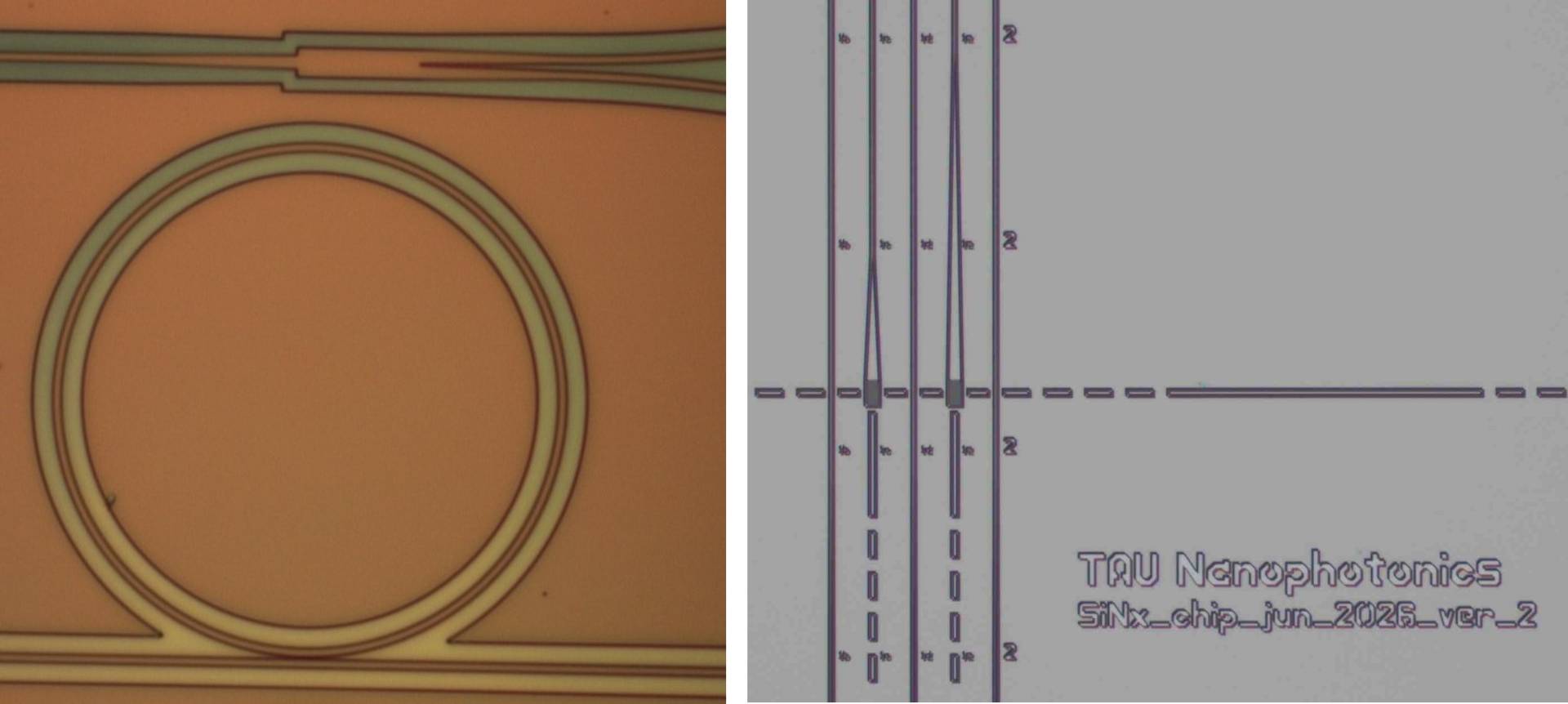
Integrated photonics circuits enables the generation, manipulation, and detection of light on microchips. By integrating optical elements such as waveguides, resonators, lasers, modulators, and detectors onto a single platform, photonic integrated circuits (PICs) can enhance performance of bulk optical elements and link with microelectronics.
Our research spans both passive and active PIC technologies. Integration of III-V semiconductor materials is investigated in collaboration with the Optoelectronics Research Centre (ORC).
At present applications range from integrated devices to generate optical vortex frequency combs to the development of ultra-sensitive micro-ring resonator sensors for biomedical imaging. Room-temperature light-matter Bose-Einstein condensates and novel photon interaction mechanisms could enable a new generation of quantum and telecom-compatible photonic circuits.
More details in Projects.
Nanomaterials and self-assembled nanostructures
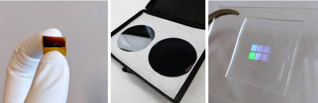
Nanomaterials with exotic properties can be created by assembling matter into complex 2D and 3D nanostructures. These materials can be used for high-resolution molecular sensing, light absorption enhancement and photon management in photovoltaic cells or as anti-reflective or self-cleaning surface coatings. The creation of nanostructured materials can be technologically challenging and one of our goals is to discover large-scale nanofabrication methods where the devices and materials “build themselves” by self-assembly.
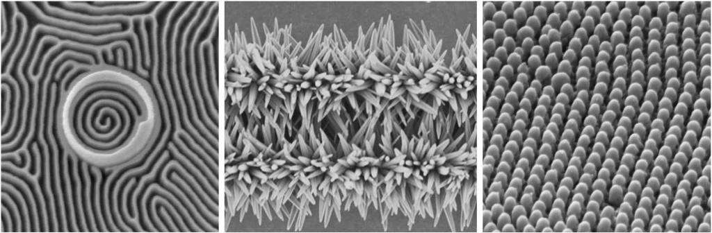
Inspired by biology, bottom-up nanofabrication approaches start from basic building blocks, such as atoms or molecules, and use them to build functional nanostructures and devices. These building blocks arrange themselves into nanostructures on their own due to physical and chemical driving forces present at the nanoscale.
We have applied block copolymer (BCP) self-assembly and hydrothermal crystal growth processes. BCPs are tailored molecules that phase-separate into small, repeating 2D and 3D patterns. We have used these patterns as templates to make light absorbing metasurfaces and nanoscopic optical resonators. See Publications for more information.
Modeling
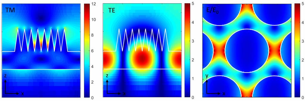
Because we cannot directly see what happens to light in the nanoscale, optical modeling is needed. Photonics tools such as Lumerical and Comsol help understand how light waves interact with the nanostructures. Modeling is an essential part of designing and verifying operation of integrated circuit elements and larger circuits.
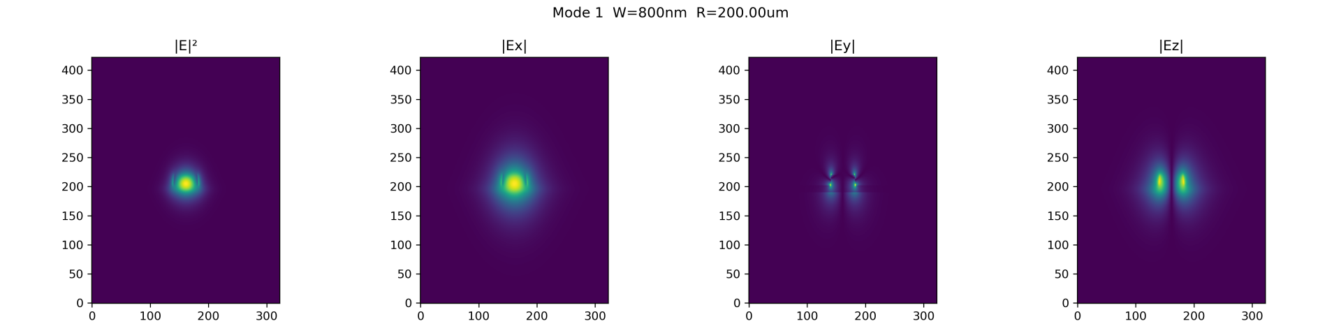
Modes in bent lithium niobate waveguide.