
High-resolution printing
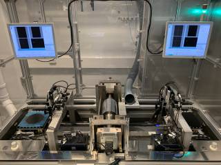
A central component of the project is the use of reverse-offset printing (ROP) for high-precision patterning of thin films. VTT has been contributing to the development of ROP towards printed and flexible electronic applications. This technique enables feature sizes at the sub-micrometer scale, significantly improving over conventional printing methods that typically operate at much lower resolution.
ROP allows patterning of materials that are not directly printable by combining printing with subsequent deposition steps. This makes it possible to fabricate fine structures required for miniaturized electronic devices, while maintaining compatibility with scalable manufacturing approaches.
The ability to achieve high-resolution patterns is essential for reducing device dimensions, improving electrical performance, and enabling more compact circuit designs.
More information on ROP process can be found on VTT’s website: https://www.vttresearch.com/en/news-and-ideas/printed-electronics-reaching-accuracy-one-micrometre

Laser-assisted atomic layer deposition
A key research focus of ROPALD at TAU is the development of laser-assisted atomic layer deposition (ALD) to enable spatially controlled thin-film growth.
In conventional ALD, films are deposited uniformly across the substrate, and additional patterning steps are required to define structures. In ROPALD, this limitation is addressed by integrating a laser directly into the deposition process. The laser provides localized energy to activate surface reactions only in selected regions, enabling area-selective deposition without the need for conventional lithography.
The role of the laser is therefore twofold:
- It enables lateral control, allowing material growth to occur only where the laser is applied
- It supports film formation at lower temperatures by supplying energy locally instead of heating the entire substrate
This localized energy input allows the formation of high-quality thin films while significantly reducing the overall processing temperature. Experimental results show that laser treatment can modify film properties such as thickness and density, indicating improved material quality at reduced thermal budgets.
Low-temperature thin-film fabrication
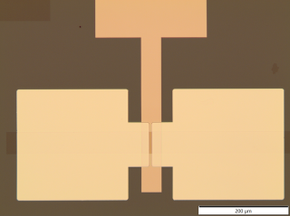
A major objective of the project is to develop thin-film device fabrication methods operating below 120 °C, focusing on developing a scalable flexible thin-film transistor process. This is significantly lower than typical processing temperatures in conventional microelectronics.
Low-temperature processing expands the range of usable substrates, including flexible plastics and potentially biodegradable materials. This enables new types of electronic systems that are lightweight, flexible, and more environmentally sustainable.
At the same time, maintaining device performance at low temperatures is a key challenge. The project addresses this by combining high-resolution patterning with advanced deposition techniques to preserve electrical properties while reducing thermal requirements.