
LFE’s state of the art printing facility includes inkjet printers (CeraPrinter F-Serie, Super-fine Inkjet printer, four Dimatix printers, of which one inside a nitrogen filled glove box and one in clean room), gravure, flexo, rotary screen and dry or wet lamination (Schläfli Challenger 174), screen printers, 3D electronics printer and a plasma printer for high resolution surface energy patterning.
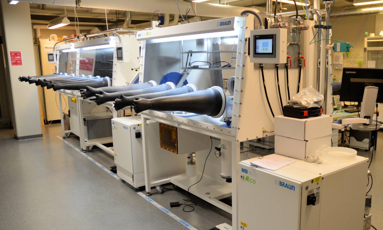
A glove box system filled with nitrogen can be used for device fabricating and characterization. The system includes integrated Dimatix inkjet printer, ALD, spin coater and vacuum hot plate as well as combined e-beam and thermal evaporator.
Equipment for electrical characterization include probe stations, semiconductor analyzer , a potentiostat and devices for measuring supercapacitors and batteries. Mechanical properties of functional materials can also be tested. Ferroelectric and piezoelectric material testing equipment is also available.
More information:
- Inkjet printers (pdf)
- Glove box (pdf)
- Flexo and gravure (pdf)
- Screen printers (pdf)
- 3D printed electronics system (pdf)
- Plasma printer (pdf)
- ALD (pdf)
- Parylene coater (pdf)
- Coating device (pdf)
- Spin coater and vacuum hot plate (pdf)
- Evaporator (pdf)
- Characterization (pdf)
- Semiconductor analyzer and Probe stations (pdf)
- Potentiostat (pdf)
- Supercapacitor and battery analyzer (pdf)
- Ferroelectric materials testing (pdf)
- Piezoelectric materials testing (pdf)
- Sheet resistance measurement (pdf)
- Other equipment (pdf)
Specialized analysis methods for e.g. microscopy and surface characterization are available through other laboratories at TAU.
Printed Intelligence Infrastructure
LFE is a part of Printed Intelligence Infrastructure (PII). PII is a distributed infrastructure between University of Oulu, Tampere University, Åbo Akademi, and VTT supported by Academy of Finland Finnish Research Infrastructure (FIRI, grant no 320017, 320019, 320020). Printed intelligence infrastructure (PII) is world-class research and development environment to researchers and technology developers in academy and industry. It offers an easy access to a modern research and pilot-manufacturing infrastructure covering the whole research/development path from materials via components and devices to circuits and systems. Available processes include synthesis of novel materials, formulation of pastes and inks, manufacturing from large-area sheet-to-sheet (S2S) and roll-to-roll (R2R) processes to hybrid integration, and finishing steps (e.g. encapsulation and 3D molding) for functional systems for internet-of-everything, diagnostics, sensors, on-skin electronics, and 5/6G.