
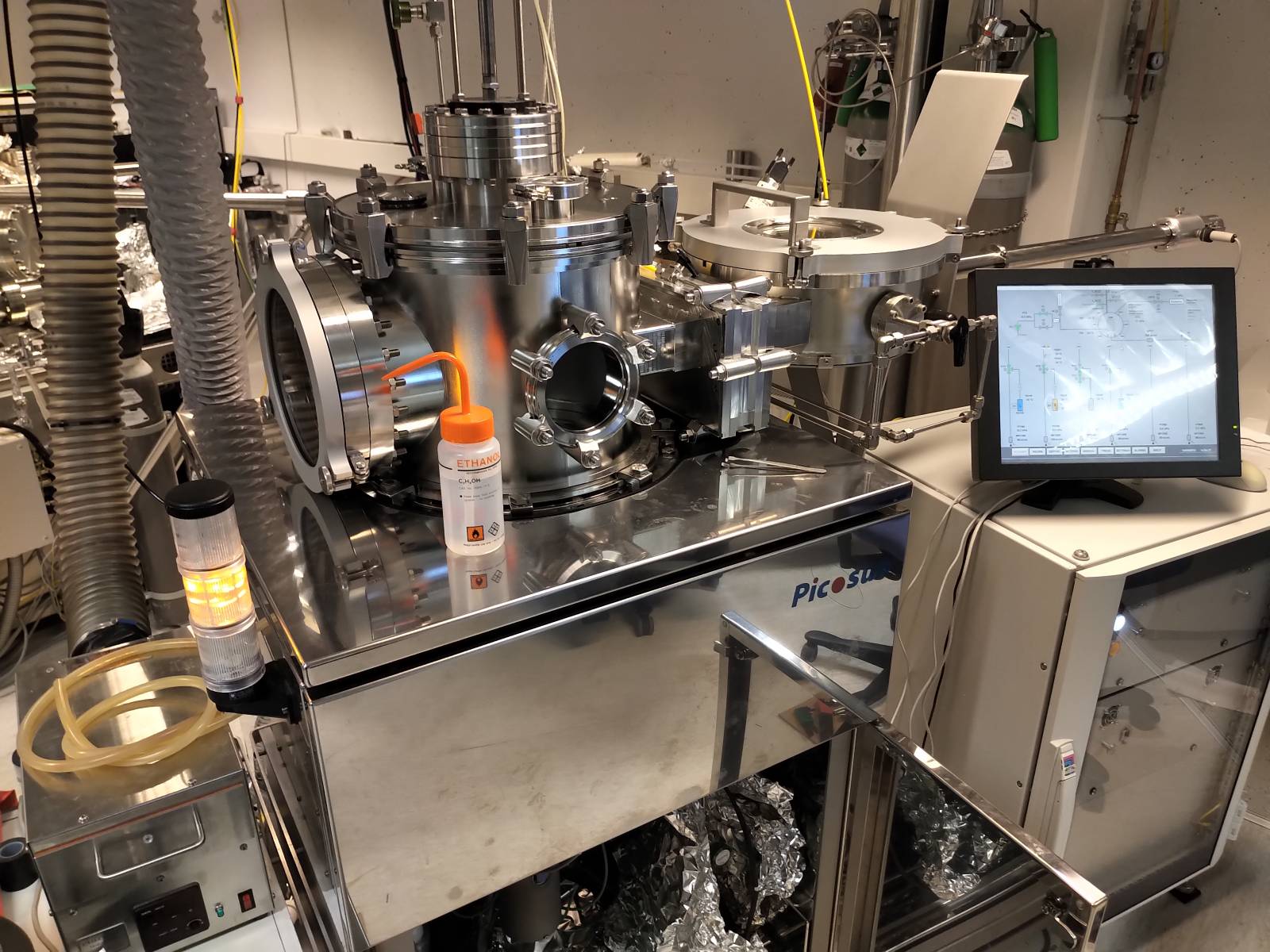
Picosun Sunale ALD R200 Advanced reactor at a glance
| Examples of materials and deposition temperatures |
|
| Sample dimensions |
|
Introduction
Atomic Layer Deposition (also known as Atomic Layering Epitaxy and Molecular Layering) was developed independently in Soviet Union in late-60s by S. I. Koltsov and V. B. Aleksovskii and in Finland in mid-70s by T. Suntola. The technique allows for growth of atomically thin films in a precisely controlled manner. ALD is based on exposing the substrate to separate pulses of gaseous precursors, which react chemically to form the desired film.
Principle of operation
ALD process is very similar to CVD (Chemical Vapour Deposition) in that a thin film is grown on a substrate in vacuum by reaction of gaseous chemicals. However, in CVD reactors all of the precursor chemicals are present in the deposition chamber at all times, while in ALD they are injected into a flowing inert carrier gas as a series of short non-overlapping pulses separated by purge periods.
During a pulse of the first precursor, the precursor adsorbs (in most cases dissociatively) onto the substrate surface. The amount of adsorbed precursor depends on the precursor-substrate interaction and much less on the time of exposure. Then the first precursor is pumped out and the second precursor is introduced to the reaction chamber. The second precursor reacts chemically with the adsorbed first precursor and a saturation layer of the product is formed. Then the excess of second precursor, along with byproducts of the reaction, is pumped out, and the process is repeated until the desired film thickness is reached. With such methodology, the amount of material deposited on the surface of the substrate is strictly defined by the self-limiting nature of precursor-substrate interaction. As a result, unprecedented control over the resulting film properties (e.g. crystallinity, refractive index, absorbance) is possible and very thin films – on the order of 0.5nm – can be reliably grown.
Applicability
ALD is very efficient at depositing thin films of materials with precisely defined properties, and that is the main application area for it. There are many precursors commercially available for use with ALD process and it has been increasingly used in academia and industry, especially in modern semiconductor manufacturing, microelectronics, and nanotechnology. ALD can therefore be used for depositing materials with novel properties as well as simply modifying the properties of the substrate in a desired manner. ALD is applicable to deposit oxides (dielectrics, semiconductors), nitrides, sulfides, III-V compounds, ternary compounds, and elements, to produce, e.g., passivation and interface layers, diffusion barriers, metallization, and antireflective coatings, including multilayered structures. Layer thicknesses from one monolayer to hundreds of nanometers can be grown to an atomically specified thickness.
One unique advantage of ALD (over CVD, PVD, and sol-gel deposition) is that the ALD process yields conformal films and even more complex shapes, e.g., vertical nanowires and inner walls of porous substrates, can be coated with uniform thin films. Furthermore, selective deposition on chemically pre-patterned surfaces is feasible by ALD.
The main disadvantages of ALD are rather slow deposition rate of typically in the order of 0.1 nm per one ALD cycle corresponding typically to ~10-50 nm/h, and limitations related to the requirements of substrate to be chemically reactive towards the precursors and resistant to the ALD process conditions, e.g., heating. The most ALD processes are operated in the temperature range of 100 to 400 °C.
Contact: Senior Scientist Kimmo Lahtonen (Kimmo.Lahtonen@tuni.fi)